|
利用AAO模板MBE外延生长Ge纳米点和薄膜
-浙江大学叶辉教授又一篇论文发表于Nanotechnology
 .jpg)
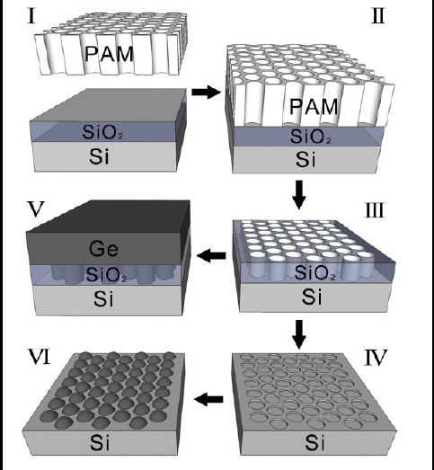
利用超薄AAO模板,首先转移到Si上,然后在Si表面刻蚀形成纳米坑阵列。高密度的Ge纳米点阵列可以通过Si纳米坑道结构的限制作用获得。高质量的Ge膜也能够通过SiO2窗口层实现。所谓SiO2窗口层是指将AAO模板转移到SiO2/Si表面,然后刻蚀在SiO2 表面形成孔阵列。比如80nm和60nm孔径的超薄AAO模板转移到SiO2/Si表面,刻蚀可以形成70, 50和20 nm孔径的窗口。通过70nm和50nm的窗口层,没有发现“threading dislocations”,主要原因是降低了晶格失配。20nm窗口层是通过一种创新的“阴影刻蚀”技术实现的。截面透射电镜结果表明,在20nm窗口层的辅助下,选择性外延生长的Ge膜没有缺陷,主要的原因是“threading dislocations”和Ge-Si之间的互扩散。
这篇论文中的所使用的AAO模板,主要是孔径80和60nm,孔深只有200-500nm(可控),是上木科技和浙江大学合作完成。
具体内容可以参考刚刚online的原文:http://iopscience.iop.org/0957-4484/24/18/185302/
Heteroepitaxy of Ge on Si(001) with pits and windows transferred from
free-standing porous alumina mask
Yourui Huangfu, Wenbo Zhan, Xia Hong, Xu Fang, Guqiao Ding
and Hui Ye*
E-mail: huiye@zju.edu.cn
Abstract
This paper reports the use of ultrathin free-standing porous alumina membrane (PAM) in pattern transferring for selective epitaxial growth (SEG) of Ge dots and films on Si. PAM, as a large-scale, controllable and lithography-free mask, can transfer nanopatterns onto Si without introducing any contaminants. High-density Ge dots are achievable with Ge adatoms confined in Si pits transferred from PAM. High-quality Ge films can also be grown on Si substrates through SiO2 nano-windows. In this work, 80 and 60 nm pore sizes of PAM were transferred to 70, 50 and 20 nm windows for comparison. For the former two sizes, over-etching of Si beneath every SiO2 window forms epi-seeds to improve intermixing of Ge–Si. No threading dislocations can be observed emanating from the epi-seeds due to the decreased lattice mismatch. An innovative shadow-etching technique utilizing the aspect ratio of PAM further decreased the lateral dimension of patterns from 60 to 20 nm. Cross-sectional transmission electron microscopy images show that the selective epitaxial Ge films grown from a 20 nm-width interface are defect free, which is attributed to the exponential decay of strain energy as well as Ge–Si intermixing.
|